Why Camera Module Performance Depends on More Than the Image Sensor
When choosing a camera module, most people focus on megapixels, sensor size, lens quality, and image-processing features. These specifications matter, but they do not tell the whole story. A camera can use an excellent image sensor and still produce disappointing results if the surrounding hardware is poorly integrated. This is where PCB fabrication and assembly becomes important, especially in camera module PCB assembly, where electronic connections, mechanical alignment, and optical performance must work together.
A Camera Module Is More Than a Sensor and Lens
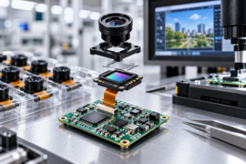
Inside a modern camera module, several components work together to capture and process images.
The image sensor converts incoming light into electrical signals. Supporting circuits provide power, timing, and communication with the main processor. Connectors or flexible circuits transfer image data to the rest of the device.
Depending on the application, the module may also include autofocus components, image stabilization hardware, or additional control electronics.
All these elements must fit into a compact structure without interfering with the optical path.
Mechanical Alignment Can Affect Image Quality
Unlike many ordinary electronic assemblies, camera modules are sensitive to physical positioning.
The relationship between the lens and image sensor influences focus and image sharpness. Even a small mechanical shift can affect optical performance, particularly in compact modules with tight tolerances.
PCB thickness, flatness, mounting features, and component placement can influence how the sensor sits within the camera housing.
However, accurate PCB assembly alone does not guarantee optical alignment. Lens positioning, adhesive curing, and optical calibration may require separate specialized processes.
The important point is that electronic and mechanical manufacturing decisions cannot always be treated independently.
Cleanliness Matters Around the Image Sensor
A tiny particle of dust may seem insignificant on an ordinary circuit board. Near an image sensor or inside an optical assembly, it can become a visible problem.
Particles, fingerprints, and contamination on optical surfaces may produce image artifacts or interfere with the final camera assembly.
This makes cleanliness particularly important during camera module production.
The appropriate controls depend on the design and assembly stage. PCB cleaning, sensor handling, protective covers, and controlled optical assembly environments may all play a role.
In camera module PCB assembly, manufacturers must also consider how soldering residues and subsequent handling could affect sensitive components.
Compact Designs Create Integration Challenges
Camera modules are commonly used in smartphones, security cameras, industrial inspection equipment, medical imaging products, and smart devices.
Many of these applications require small circuit boards with dense component placement.
Fine-pitch connectors, miniature passive components, image sensors, and flexible PCB connections may occupy very limited space. At the same time, the module must connect securely to the main device.
A compact design therefore needs to balance electrical performance, mechanical clearance, assembly access, and connector reliability.
Image Quality Can Reveal Hardware Problems
Not every camera problem originates in the lens or image-processing software.
Unstable power supplies, poor electrical connections, or signal transmission problems may contribute to image noise, intermittent operation, or communication errors.
For example, a camera may work normally during initial testing but experience occasional frame loss when the device operates under different conditions.
Troubleshooting these problems requires engineers to examine the complete system rather than immediately assuming that the sensor itself is defective.
This is another reason why consistent PCB fabrication and assembly matters for imaging hardware.
Camera Testing Should Go Beyond Power-On
A camera module that powers on successfully is not necessarily ready for use.
Depending on the product, verification may involve checking image capture, communication interfaces, power stability, and operation under different conditions.
Optical performance may also require dedicated checks for focus, image defects, or alignment after the module has been integrated with its lens and housing.
These tests serve different purposes. Electrical testing confirms that the electronics function correctly, while optical testing evaluates whether the complete camera system produces acceptable images.
Both contribute to the final user experience.
Conclusion
A good camera module is not defined by its image sensor alone. Mechanical positioning, cleanliness, electrical connections, power stability, and optical integration all influence how the finished product performs.
Reliable camera module PCB assembly provides the electronic foundation for these functions, while controlled PCB fabrication and assembly helps maintain the physical and electrical characteristics required by compact imaging hardware.
The result is not simply a circuit board that works, but a camera system better prepared to deliver the image quality its design was intended to achieve.